Do you mean that you found a store selling simple copies of my board, against
my wishes, or that you took my Gerbers and had a board house make some for you, in accord with my wishes?
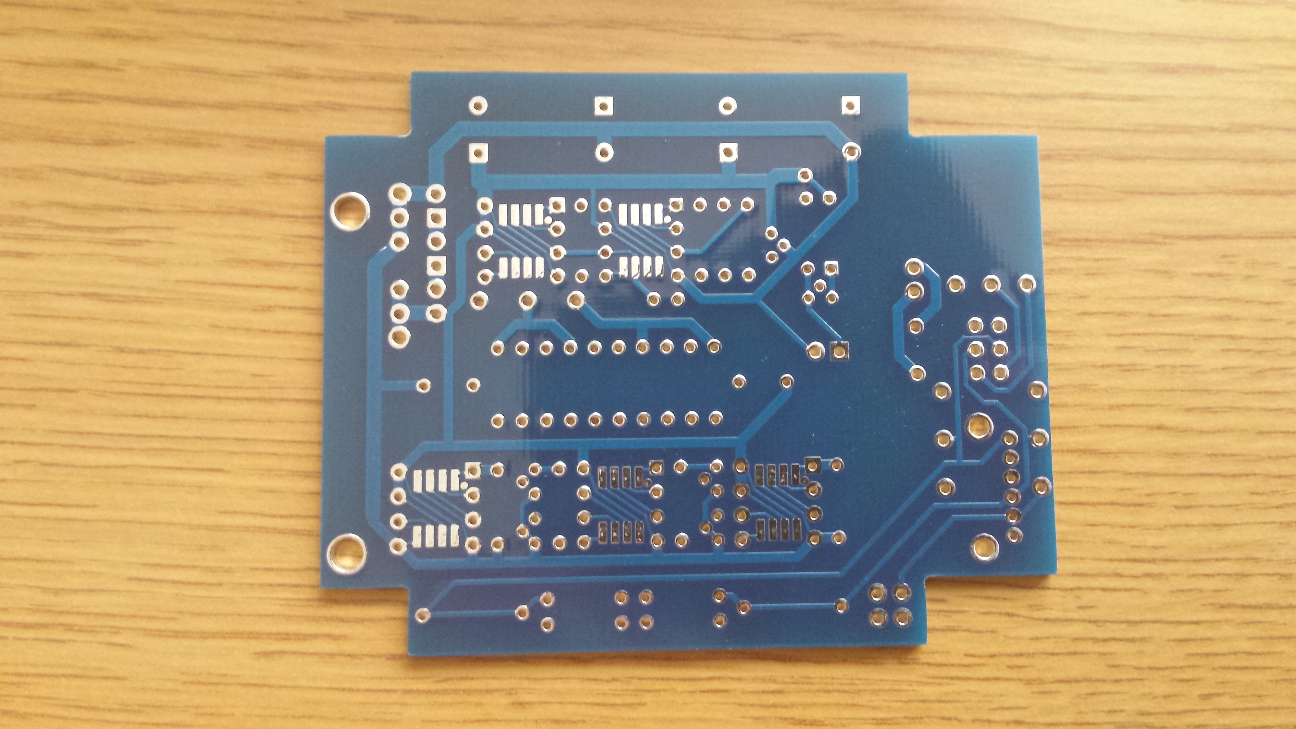
If the latter, did you tell them it needs to be a 4-layer board? If you made it as a 2-layer copper board, that'll explain a whole lot of trouble.
Your close-up photo of one of the buffers (BUFR?) shows a number of problems with the physical realization of these boards relative to an original I've got sitting around here still:
- Pin 4 appears completely flooded, not fenestrated into the plane.
- The originals don't have those thin fingers between the pins, most egregiously between 2&3, and between 6&7.
- Whoever ordered the boards elected not to include the bottom side silk layer, which means you might not be populating the components in the right spots or in the right orientation
Observations 1 & 2 call into question whether these boards do in fact express the schematic correctly. What other creepage and tolerance problems are there, which could cause shorts, opens, and parasitics where we don't want them? I've made
a close-in screenshot of what my Gerber viewer shows for BUFR in the bottom copper layer, which I believe is what you're showing in the second picture.
Quelle différence!
Observation 3 means we're reliant on your photos to tell whether your buffers are oriented correctly on their pads. It
looks like two of your buffers are oriented on the pads correctly; you don't show the third.
Moving onto check the IG to Outputs revealed some scary results:
What op-amps are you using? Maybe post pictures.
I checked the output of pins 1 & 5 - again, perfect, and absolutely in line with my gain settings. So, I decided to solder 1 of the buffers into place.
I don't see how your op-amp tests gave sensible results without the buffers in place, especially the gain, since that means you'd be running on the inner Jung loop, which has a gain far higher than you'd be expecting.
Unless you shorted the buffer positions, you should
not have gotten sensible results from that test.
Pin 2 of the output buffer goes to R11 - I carefully made sure that Pin2 did indeed go to R11 (currently unpopulated), soldered down the legs and re-checked. Now, output from the corresponding OPALR Pin 1 is near zero,
I can't tell whether this is a grammar error — should these be two separate paragraphs? — or you're trying to get some point across to us that I'm missing. There's nothing about sentence 1 that leads us to sentence 2, and sentence 2 doesn't in any way clarify sentence 1.
OPALR pin 1 is a signal output pin, and BUFL pin 2 is a power modifier. You would not expect any connection between them, nor is there supposed to be.
I believe something to be amiss with the buffers
Did you get them from a reputable source?
Maybe someone who's bought some of these recently could tell you whether they're still marking these chips with the Nat Semi logo so many years past their absorption into TI. Mine are so-marked, but they're from before the merger.
any other pointers you may have.
The board could use
a cleaning. It wouldn't be the first time I saw that solve a problem.


")
 almface:
